Cache in Computer Architecture

Cache
The concept of cache began when the memory bandwidth did not scale well with the speed of the processor and the size of the memory. In other words, the memory bandwidth is bottlenecked because the processor can execute at high speed, and it needs high-speed data to execute as well. Therefore, the cache is introduced between the memory and processor. To define more clearly, the memory here means the off-chip memory, which is basically DRAM since it is large and slow compared to the on-chip memory. Cache, on-chip memory, is designed to be a buffer between these two. The analogy of cache is similar to when you want to read some books from the library, and the cache is considered your bookshelf. Provided that you want to read some books, you then search for that book on your shelf. If you cannot find a book, you must go to the library to take it. Doing so, the library is considered a memory, and the path between your house and the library is as long as the path from the processor to memory. In short, caches provide a memory illusion between the processor and the real memory.
Cache is built with the principle of locality, which are temporal and spatial locality. The temporal locality claims that if a memory location is taken, it will then tend to be taken again in the near future. Meanwhile, the spatial locality claims that the memory location taken tends to be taken soon. Based on these concepts, the cache would build in a hierarchy, normally in 2 levels named L1 cache and L2 cache. The L1 cache would be as fast as possible, but it would be more expensive and thus smaller, while the L2 cache would be a bit slower, cheaper, and larger.
Building a cache
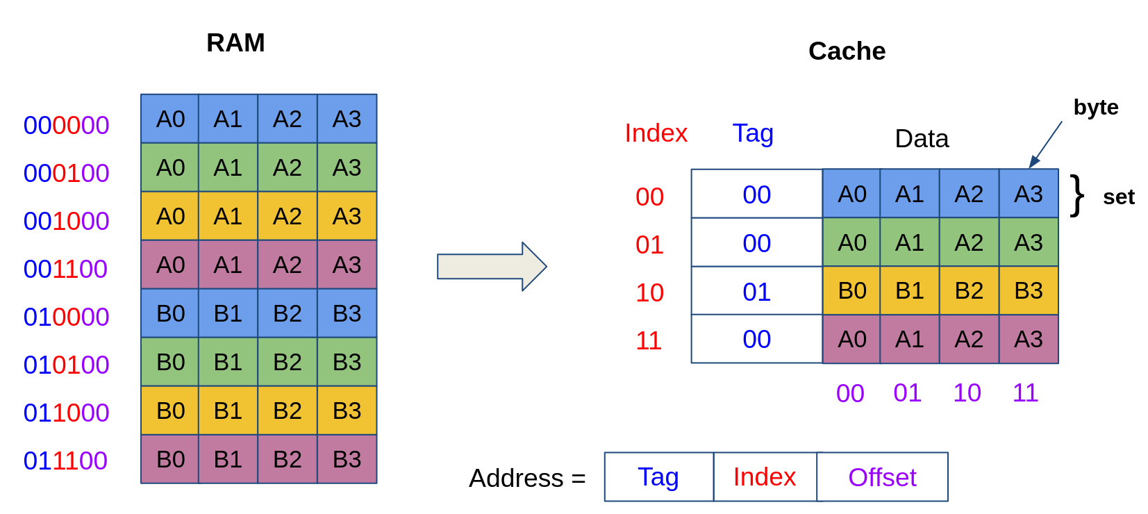
Cache normally uses the word block, which is the unit of transfer between memory and cache. The block would be larger than bytes of words, and the size of the block is specified in the design. Each block has an offset to specify the data in the block. There is an index to divide the data into a set as well as the tag that identifies which memory block is current in each cache slot. To prevent grabbing garbage data, the cache has a valid bit to ensure the validity of data.
To design a cache, firstly, we must design the block size, which is the number of data that can be stored in one block. The address in the block would be divided into tag and offset. The offset bit is the lower \(\log_2(\text{block_size})\) bits of the address, and the rest of that is a tag. For example, assume we have a 32-bit address and we have an 8-byte block. Thus, the lower 3 bits specified that the offset and rest ([31:3]) are tags.
Fully Associative Cache
A fully associative cache considers that each memory block can map anywhere in the cache. This is very efficient, but it consumes costly resources when it needs to check. It needs to check all the cache slots in sequence. If the valid bit is one and the tag matches, the data corresponding with the offset must be returned. The memory address field for fully associative cache is only tag and offset, where offset is the lower \(\log_2(\text{block_size})\) bits.
To utilize cache, basically the processor fetches the address to the cache. There are two scenarios that can happen: cache hit and cache miss. If it hits (the valid one and tag match), the cache returns the desired data. If it misses (valid is zero or tag mismatches), cache fetches the address to the memory and returns back simultaneously with storing that data to cache. If the cache is full, the cache controller must evict one valid block and replace it with desired data, which normally complies with Least-Recently Used (LRU).
The components in the cache:
- The number of slots (cache size/K)
- Each slot contains the actual data blocks.
- The tag field as identifier
- The valid bit
- Management bits (LRU bits)
The total bit in cache is \(\#slot \times (n2^{\text{offset}} + \text{tag} + \text{mbit})\) where #slot refers to the number of slots, which is the size of the cache divided by the block size, and offset and tag refer to the number of offset and tag bits, respectively. The mbit refers to some fancy attribute of cache. The n refers to the width of data for each offset of the block. For example, we have a fully associative cache with a memory space of 64B, a block size of 1 word, a cache size of 4 words, and it has 2 bits for LRU.
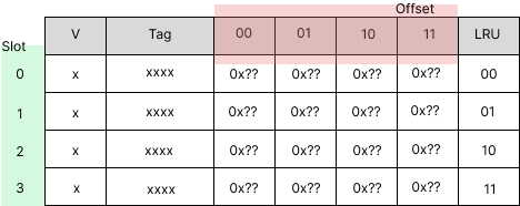
Therefore, we have \(\#slot = 4/1 = 4\). Since the block size is 1 word or 4 bytes, the offset is \(\log_2(4) = 2\). Since the address space is 64B, which can fit 6 bits of address, the tag bit is the rest of the space, which is 4. In total, we have \(4\times(8 \times 2^2 + 4(\text{tag}) + 1(\text{valid}) + 2) = 156\) bits. The figure shows the cache field, which consists of 4 slots, and each slot contains a 32-bit block and 7 auxiliary bits (39 bits in total).
Fundamentally, cache should be read and written. However, the read and write policy is independent. Reading policy is done by checking the tag, while writing policy is done by writing the data to cache only, then updating memory when the block is evicted. To do this, the dirty bit is introduced in the management bit to represent the block being written and needing to be written back to the memory. However, if the write is missed, we have to write to the memory directly simultaneously with updating the cache, namely the write-allocate policy.
Direct-Mapped Cache
Since the fully associated cache has the disadvantage that it needs to check all the tags in the cache, the direct map check is just only one slot for the block, which is much faster. In the direct-mapped, every memory block has only one home in the cache block. Direct-mapped cache utilizes an index field to specify the cache index, which is the slot of the cache we should look at. The index field is the number of slots in the cache, which is the cache size divided by the block size. It remains the same offset and tag field as a fully associated cache. The component of direct-mapped cache is shown:
- Block of data
- Tag field
- Valid bit
- Dirty bit
- Replacement bit (management bit)
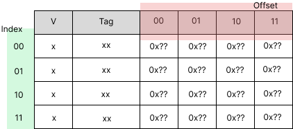
Therefore, the total bits in cache is \(\#slot \times (n2^{\text{offset}} + \text{tag} + \text{mbit})\). For example, we have a memory space of 64B, a block size of 4B, a cache size of 16B, and write-through. Since the block size is 4B, then the offset would be the logarithm base 2 of 4B, which is 2. Then, the number of slots is defined as cache size divided by block size; here it is 16/4 = 4. Therefore, the index bit is also the logarithm base 2 of the slot, which is also 2. Lastly, the tag is the rest bit, which is 2 as well. In total, the bits in the cache are 140 bits. This cache is shown in the figure above, and it has 35 bits per index/slot. The index of the direct-mapped cache is static and will not change since it specifies the location of where the memory block can be located. For example, address 0000XX can be mapped to index 00 as well as 0100XX, 1000XX, and 1100XX, where XX is a don’t care bit. These scenarios are shown in the figure below [1].
Set-Associative Cache
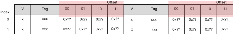
Instead of pointing to a slot, we can point to a set. Therefore, the index is a little bit changed from \(I = \log_2(C/K)\) to \(I = \log_2(C/K/N)\) where K is the block size and N is an associative set. For direct mapped, N is equal to one. For example, we want to design a 2-way set associative with a 64B memory address, a 1-word block size, a 4-word cache size, and write-through. We will have C/K/N set, which is 2 sets. Then, we have an offset of \(\log_2(4)=2\), an index of \(\log_2(2)=1\), and a tag of \(6-1-2=3\). The cache field is shown in the figure below. It can be seen that it has 37 bits per slot, 74 bits per set, and 148 bits to implement.
In a set-associative cache, the memory block can be mapped to the n block location in the cache. The n here represents the set. In general, the memory address that has the same index can be mapped only in the corresponding set.
Measuring Memory Access
The average memory access time (AMAT) defines the average time to access memory that considers both hits and misses. It calculates as \(AMAT = HT + MR \times MP\) where HT, MR, and MP are hit time, miss rate, and miss penalty. The hit time is the timeto check in cache. The miss rate is the percentage of accesses of a program that are not in the cache when we want the data. The missed penalty is the cost that we need to go down to another hierarchy to get the data.
There are two ways to reduce AMAT: decrease MR and MP. To reduce the miss rate, there are 3 Cs to consider: compulsory, capacity, and conflict. The common ways are to increase the block size of the cache or increase the cache size. We can increase associativity, which might increase hit time as well. We can reduce miss penalty by introducing cache hierarchy. The memory that is close to the processor tends to have a low hit time, while a little bit further tends to focus on a low miss rate. When we have multilevel cache AMAT, we will have \(AMAT = L1\_HT + (L1\_MR \times L1\_MR)\) where \(L1\_MR = L2\_HT + (L2\_MR \times L2\_MP)\).
Reference
[0] David A. Patterson, John L. Hennessy. 2021. Computer Organization and Design RISC-V Edition The Hardware Software Interface. The Morgan Kaufmann Series in Computer Architecture and Design.
[1] https://cass-kul.github.io/exercises/7-cache/
Related Posts: